
TOLT and TSPAK Top-Side Cooling Packages for SiC MOSFETs and SBDs
News | 2025-11-14
Follow Us
-
 LinkedIn
 -
 WeChat
TOLT and TSPAK Top-Side Cooling Packages for SiC MOSFETs and SBDs
The adoption of silicon carbide (SiC) MOSFETs and Schottky barrier diodes in high-power systems such as automotive, PV arrays and data centers has highlighted limitations of traditional surface-mount packages.
Traditional surface-mount packages use bottom-side cooling, where heat passing through the circuit board creates a thermal bottleneck and limits the performance and reliability of the advanced SiC components. Top-side cooled (TSC) packages dissipate heat directly from the top of the package into a heatsink, bypassing the PCB entirely.
TOLT and leaded TSPAK offer significant advantages, including superior thermal management and reduced EMI.
The enhanced cooling allows for the use of smaller, less expensive SiC chips to achieve the same performance as larger dies in traditional packages.
1. What are top-side cooled packages
Advances in wide bandgap technologies, particularly silicon carbide (SiC) MOSFETs and Schottky barrier diodes (SBDs) have created a significant thermal management challenge.
While these fast-switching components offer significant efficiency, power delivery and power density benefits versus silicon, and have a much higher operational temperature range, SiC MOSFETs and SBDs still concentrate substantial heat within a very small die area.
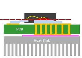
Traditional surface-mount SiC packages have relied on bottom-side cooling, with heat dissipated into the PCB, which is a poor thermal conductor, before reaching the heatsink.
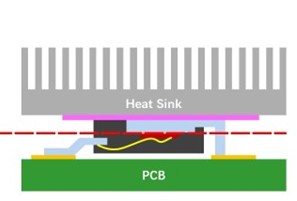
To prevent this thermal bottleneck and the limits it creates for performance/reliability, packages using top-side cooling have been developed. In these, heat is dissipated directly from the top of the package into a heatsink and enables SiC devices to operate at their full potential.
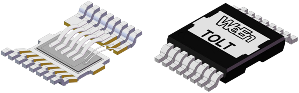
The key top-side cooling packages are TOLT (TO-leadless top-side cooling) and TSPAK (TO-leaded small-outline package).
2. Legacy technologies
The electrification of transport, coupled with the increased power delivered by wind/solar facilities, the need for improved efficiencies in all systems, and the rise of exceptionally high-power applications such as data centers, has meant a shift to wide bandgap materials, particularly SiC.
SiC has an ultra-low VF and on-state resistance (RDSon), resulting in efficient power conversion and reduced losses.
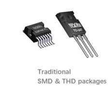
Compared to traditional through-hole devices (THD), the primary advantage of a top-side cooled package (TSC) is its suitability for highly automated PCB assembly. As a surface-mount package, TSC devices eliminate the manual labor associated with through hole mounting and screw tightening, thereby reducing costs and improving manufacturing consistency.
Traditionally, surface mount packages such as D2PAK (TO-263), DPAK (TO-252), TOLL (TO Leadless) and DFN (Dual Flat No-lead) dissipated heat through the package and into the PCB and spreading it, or transferring it to a heatsink.
3. Topside-cooled packages
3.1 TOLT
3.1.1 Design and construction
The TOLT is a leadless surface-mount package with bottom-side pads for soldering to a PCB. It implements a large, exposed metal plate on its top surface. This plate is thermally connected to the die. This creates a highly efficient thermal path that bypasses the PCB entirely.
The package is therefore used in applications with significant requirements for thermal management.
3.1.2 Performance and electrical characteristics
The package provides a direct, low-resistance path from the semiconductor junction to the heatsink, significantly reducing junction-to-case thermal resistance (R_thJC).
The leadless design also reduces package parasitic inductance to enable the ultra-fast switching speeds of SiC devices to be implemented. Voltage overshoot and ringing are also reduced as a result of the package’s low inductance. In doing so, cleaner switching waveforms are enabled with lower switching losses, and reduced EMI.
Many TOLT devices also include a Kelvin source pin to further optimize gate drive performance.
3.2 TSPAK
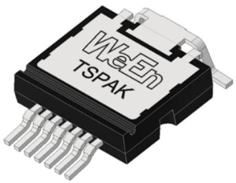
3.2.1 Design and construction
TSPAK is a leaded top-side cooled surface-mount package with electrical connections made via gull-wing leads that are soldered to the PCB. Its large, exposed metal plate is thermally connected to the die for direct mounting to a heatsink.
3.2.2 Performance and electrical characteristics
Like the TOLT, the TSPAK's top-side cooling design provides excellent thermal performance, enabling the use of smaller, more cost-effective SiC chips. Both packages offer low circuit inductance compared to traditional designs. TSPAK’s leaded design is slightly more prone to parasitic inductance than TOLT, with the package also optimizing for lower costs and increased robustness in high-performance applications.
3.3 EMI benefits of top-side cooled packages
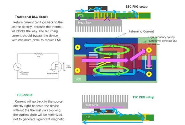
Magnetic fields are generated by current loops, with larger loops generating stronger magnetic fields and increasing the risk of EMI. As such, it’s important to keep the supply and return current paths as close together as possible, and thereby minimizing the area of any high-frequency alternating magnetic field.
Bottom-side cooled packages often rely on thermal vias drilled through the circuit board directly under the component to dissipate heat. This is effective for cooling, but prevents a direct return path for the current on the ground plane and creates a large bypass loop around the component. The AC magnetic field area therefore cannot be reduced, and significant EMI noise levels are generated.
This is solved in top-side cooled packages, with the thermal path moved off the PCB entirely meaning the return current can travel directly beneath the device and thereby minimize the current loop’s size.
Magnetic field emission is therefore significantly reduced in TOLT and TSPAK packages, leading to lower overall EMI.
3.4 Cost benefits of top-side cooled packages
The thermal performance offered by TOLT and TSPAK packages enables the use of smaller, more cost-effective SiC chips to deliver the same performance as a larger, more expensive SiC device in a traditional package.
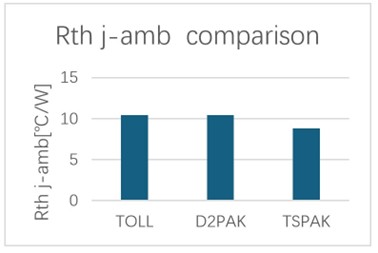
This cost saving can be seen if we compare the performance of a 60 mΩ SiC D2PAK device versus a comparable TSPAK device running with a junction temperature of 87oC / ambient temperature of 25oC. In this scenario, the D2PAK device has a thermal resistance (RTHj-amp) of 10.4 K/W, and a power dissipation of P=5.96 W supports a current of 9.967 A.
The reduced thermal resistance offered by the TSPAK device running at the same temperatures and with the same current enables a lower RTHj-amp of 8.8 K/W. As a result, P increases to 7.045 W allowing a TSPAK MOSFET and thereby allowing a device with an RDson of 70.9 mΩ (P/I) to be used.
By using a 71 mΩ TSPAK over a 60 mΩ D2PAK, cost savings will be in the region of 15-20%.
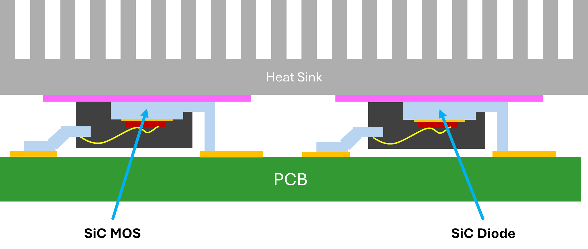
3.5. TSC packages in combined MOSFET and diode circuits
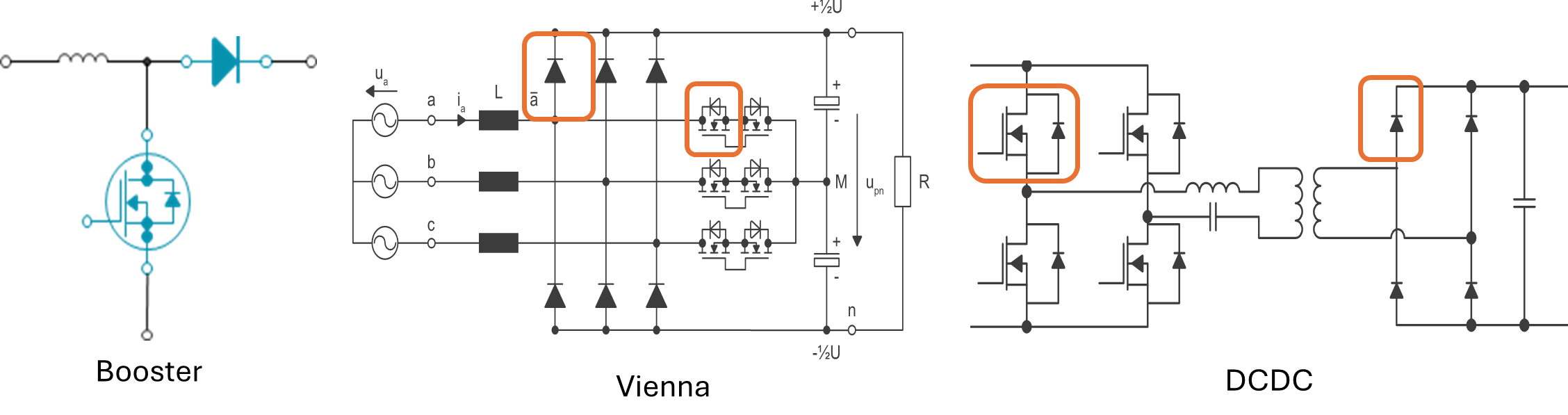
Many commonly used topologies rely on a combination of MOSFETs/diodes working together. For example, this can be seen in Vienna PFC, and the primary and secondary sides of LLC converters.
For effective thermal management, these components often need to be mounted on a single, shared heatsink. To enable this and simplify the mechanical layout and thermal design significantly, WeEn makes both SiC MOSFETs and diodes available in the same TOLT and TSPAK formats. This makes it much easier for engineers to adopt and implement these advanced packages into new, high-density power solutions.
4. Applications
4.1 Applications for TOLT packages
The TOLT package’s thermal performance properties, coupled with its low inductance, makes it ideally suited to more demanding applications where maximizing power density and efficiency is critical. These include:
4.1.1 Automotive:
EV traction invertersOn-board chargers (OBC) High-voltage DC-DC converters48V mild-hybrid (MHEV) systems
4.1.2 Industrial:
PV InvertersIndustrial motor drivesUninterruptible power supplies (UPS)
4.1.3 Telecommunications and data centers:
High-power density PSUs for servers and AI accelerators 5G base stations
4.1.4 EV charging infrastructure:
Public super chargers (40-60kW) Household DC chargers (7-22kW)
4.2 Applications for TSPAK packages
The presentation strongly positions the TSPAK package for automotive and charging applications due to its high-power density and design flexibility.
4.2.1 Automotive:
On-board chargers (OBC) E-compressors High-voltage DC-DC convertersEV traction inverters
4.2.2 Industrial:
High-efficiency solar invertersIndustrial motor drives
4.2.3 EV Charging infrastructure:
Public super chargers (40-60kW) Household DC chargers(7-22kW)
5. WeEn TOLT and TSPAK products
WeEn Semiconductors offers 650 V TOLT packaged SiC products for use across a wide range of industrial and automotive applications. Its MOSFETs are available with an RDSon of between 20 and 70 mΩ. Its Schottky barrier diodes (SBDs) are available for currents of 10~20 A.
WeEn’s Semiconductors’ TSPAK packaged SiC products are available for both 650 V and 1200 V, with its MOSFETs available with an RDSon range between 12 and 150 mΩ and its SBDs available for currents 10 to 40A.
6. WeEn offering and announcements
Note – to be used to link to specific announcements and pages