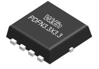
WMS20N270SE is a high performance super logic level N-channel MOSFET in PDFN3.3X3.3 package, which utilizes advanced Trench MOSFET technology to provide low RDS(on) and gate charge. It is designed and qualified in a wide range of industrial and consumer applications.
- Advance High Cell Density Trench Technology
- Low RDS(on) to Minimize Conduction Losses
- Low Capacitance to Minimize Switching Losses
- Optimized Gate Charge to Minimize Driver Losses
- 100% UIS Tested
- RoHS Compliant, Halogen Free and Lead Free
- DC−DC Converters
- BLDC Motor Control
- Load Switch
- Lithium-ion Battery Protection
| Type Number | Symbol | Parameter | Conditions | Min | Typ/Nom | Max | Unit |
| WMS20N270SE | VDS | drain-source voltage | 20 | V | |||
| VGS | gate-source voltage | ±10 | V | ||||
| ID | drain current | VGS = 4.5 V; Tmb = 25 °C | 18 | A | |||
| Ptot | total power dissipation | Tmb = 25 °C | 14 | W | |||
| Tj | junction temperature | -55 | 150 | °C | |||
| RDS(on) | drain-source on-state resistance | VGS = 4.5 V; ID = 8 A | 17 | 27 | mΩ | ||
| VGS = 2.5 V; ID = 3 A | 25 | 44 | mΩ | ||||
| QG(tot) | total gate charge | ID = 8 A; VDS = 10 V; VGS = 4.5 V | 5.1 | nC |
| Type number | Package | Packing | Product status | Marking | Orderable part number | Ordering code (12NC) |
|---|---|---|---|---|---|---|
| WMS20N270SE |
PDFN3.3X3.3 |
STANDARD MARK SMD | Volume production | Standard Marking | WMS20N270SEJ | 9340 733 66118 |
| Type number | Ordering code (12NC) | Orderable part number | Region | Distributor | Order sample |
|---|---|---|---|---|---|
| WMS20N270SE | 9340 733 66118 | WMS20N270SEJ | NA | NA |
| Chemical content | Orderable part number | Type number | RoHS / RHF | Leadfree conversion date | MSL | MSL LF |
|---|---|---|---|---|---|---|
| WMS20N270SE | WMS20N270SEJ | WMS20N270SE |  |
always Pb-free | 1 |
Chemical Content - WMS20N270SE
Disclaimer
All information in this document is furnished for exploratory or indicative purposes only. All information in this document is believed to be accurate and reliable. However, WeEn Semiconductors does not give any representations or warranties as to the accuracy or completeness of such information and shall have no liability for the consequences of use of such information. WeEn Semiconductors may make changes to information published in this document at any time and without notice. Minor deviations may occur in the products from different manufacturing location. This document supersedes and replaces all information supplied prior to the publication hereof. Nothing in this document may be interpreted or construed as an offer to sell products that is open for acceptance or the grant, conveyance or implication of any license under any copyrights, patents or other industrial or intellectual property rights.


