
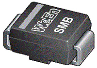
P6SMBJ series, 600W transient voltage suppressor (TVS) in SMB package, designed to protect electronic circuits against damage induced by lightning surges or other transient voltage events.
- Peak pulse power 600W @ 10/1000μs waveform
- Excellent clamping capability
- Low incremental surge resistance
- Surface mount package for easy assembly and PCB space-saving
- Typical IR < 1μA when VBR min > 12V
- Fast response time: typically < 1.0ps from 0V to VBR minimum
- IEC 61000-4-2 ESD 30kV (Air), 30kV (Contact)
- EFT protection of data lines in accordance with IEC 61000-4-4
- Guaranteed high temperature for reflow soldering: 260°C/10sec
- Mold compound complies to UL94V-0 flammability classification
- Meets MSL level 1, per J-STD-020
- Pb-free lead finish
- Halogen free and RoHS compliant
- Power supplies
- Industrial applications
- Power management circuits
- I/O interfaces
| Type Number | Symbol | Parameter | Conditions | Min | Typ/Nom | Max | Unit |
| P6SMBJ17A | VR | reverse stand off voltage | 17 | V | |||
| VBR | breakdown voltage | IT = 1 mA | 19.08 | 20.72 | V | ||
| Tj | junction temperature | -65 | 150 | °C | |||
| VC | clamping voltage | IPP = 21.8 A; tp = 10/1000 μs | 27.6 | V | |||
| IPP | peak pulse current | 10/1000μs waveform | 21.8 | A | |||
| IR | reverse leakage | VR = 17 V | 1 | μA |
| Type number | Package | Packing | Product status | Marking | Orderable part number | Ordering code (12NC) |
|---|---|---|---|---|---|---|
| P6SMBJ17A |
SMB |
STANDARD MARK SMD | Volume production | Standard Marking | P6SMBJ17AJ | 9340 731 13118 |
| Type number | Ordering code (12NC) | Orderable part number | Region | Distributor | Order sample |
|---|---|---|---|---|---|
| P6SMBJ17A | 9340 731 13118 | P6SMBJ17AJ | NA | NA |
| Chemical content | Orderable part number | Type number | RoHS / RHF | Leadfree conversion date | MSL | MSL LF |
|---|---|---|---|---|---|---|
| P6SMBJ17A | P6SMBJ17AJ | P6SMBJ17A |  |
1 | 1 |
Chemical Content - P6SMBJ17A
Disclaimer
All information in this document is furnished for exploratory or indicative purposes only. All information in this document is believed to be accurate and reliable. However, WeEn Semiconductors does not give any representations or warranties as to the accuracy or completeness of such information and shall have no liability for the consequences of use of such information. WeEn Semiconductors may make changes to information published in this document at any time and without notice. Minor deviations may occur in the products from different manufacturing location. This document supersedes and replaces all information supplied prior to the publication hereof. Nothing in this document may be interpreted or construed as an offer to sell products that is open for acceptance or the grant, conveyance or implication of any license under any copyrights, patents or other industrial or intellectual property rights.