
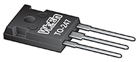
WG50N65MFW1 uses advanced Fine Trench Field-stop IGBT technology with anti-parallel diode in TO247 package to provide extremely low VCE(sat), and excellent switching performance. This device offers Best-in-Class efficiency in hard switching and resonant topology.
- Maximum junction temperature 175 °C
- Positive Temperature efficient for easy paralleling
- Very soft, fast recovery anti-parallel diode
- Smooth & Optimized switching
- EMI Improved Design
- Motor control
- PFC
- UPS
- Resonant converters
- Mid to high switching frequency applications
| Type Number | Symbol | Parameter | Conditions | Min | Typ/Nom | Max | Unit |
| WG50N65MFW1 | VCE | collector-emitter voltage | 650 | V | |||
| IC | collector current | TC = 25 °C | 100 | A | |||
| IF | diode forward current | TC = 25 °C | 100 | A | |||
| VCE(sat) | collector-emitter saturation voltage | VGE = 15 V; IC = 50 A; Tj = 25 °C | 1.55 | 1.95 | V | ||
| VF | diode forward voltage | VGE = 0 V; IF = 50 A; Tj = 25 °C | 2 | V | |||
| VGE(th) | gate-emitter threhold voltage | IC = 0.5 mA; VCE = VGE | 4.3 | 5.4 | 6.5 | V | |
| Qg | gate charge | VCC = 520 V; IC = 50 A; VGE = 15 V; Tj = 25 °C | 133 | nC | |||
| Eon | turn-on energy | Tj = 25 °C; VCC = 400 V; IC = 50 A; VGE = 15V / 0V; RG = 10 Ω | 1.38 | mJ | |||
| Eoff | turn-off energy | 0.72 | mJ | ||||
| Qr | reverse recovery charge | Tj = 25 °C; VR = 400 V; IF = 50 A; dIF/dt = 500 A/us | 321 | nC |
| Type number | Package | Packing | Product status | Marking | Orderable part number | Ordering code (12NC) |
|---|---|---|---|---|---|---|
| WG50N65MFW1 |
TO247 |
HORIZONTAL, RAIL PACK | Volume production | Standard Marking | WG50N65MFW1Q | 9340 738 29127 |
| Type number | Ordering code (12NC) | Orderable part number | Region | Distributor | Order sample |
|---|---|---|---|---|---|
| WG50N65MFW1 | 9340 738 29127 | WG50N65MFW1Q | NA | NA |
| Chemical content | Orderable part number | Type number | RoHS / RHF | Leadfree conversion date | MSL | MSL LF |
|---|---|---|---|---|---|---|
| WG50N65MFW1 | WG50N65MFW1Q | WG50N65MFW1 |  |
NA |
Chemical Content - WG50N65MFW1
Disclaimer
All information in this document is furnished for exploratory or indicative purposes only. All information in this document is believed to be accurate and reliable. However, WeEn Semiconductors does not give any representations or warranties as to the accuracy or completeness of such information and shall have no liability for the consequences of use of such information. WeEn Semiconductors may make changes to information published in this document at any time and without notice. Minor deviations may occur in the products from different manufacturing location. This document supersedes and replaces all information supplied prior to the publication hereof. Nothing in this document may be interpreted or construed as an offer to sell products that is open for acceptance or the grant, conveyance or implication of any license under any copyrights, patents or other industrial or intellectual property rights.