The ESDALD05BE2 is a low capacitance TVS (Transient Voltage Suppressor) array designed to protect high speed data interfaces.
It is available in bi-directional configurations and is rated at 300 Watts for an 8/20 μs waveshape.
- Peak pulse power 300W @ 8/20μs waveform
- IEC 61000-4-2 ESD 30kV (Air), 30kV (Contact)
- Protect one bidirectional line or two unidirectional lines
- Low capacitance
- Low clamping voltage
- Low leakage current
- Meet MSL level1
- Halogen free and RoHS compliant
- Mobile phones & accessories
- Portable Electronics
- Computers and peripherals
- Microprocessor based equipment
- Personal Digital Assistants (PDA)
- Networking and Telecom
- Serial and Parallel Ports
| Type Number | Symbol | Parameter | Conditions | Min | Typ/Nom | Max | Unit |
| ESDALD05BE2 | VR | reverse working voltage | 5 | V | |||
| VBR | reverse breakdown voltage | IT = 1 mA | 6.5 | 9.6 | V | ||
| Tj | junction temperature | -55 | 150 | °C | |||
| VC | clamping voltage | IPP = 1 A; tp = 8/20 μs | 9.5 | V | |||
| IPP = 15 A; tp = 8/20 μs | 21 | V | |||||
| IPP | peak pulse current | 8/20μs waveform | 15 | A | |||
| IR | reverse leakage current | VR = 5 V; pin 1/2 to pin 3 or pin 3 to pin 1/2 | 200 | nA | |||
| Cj | Junction Capacitance | VR = 0 V; f = 1 MHz; | 0.5 | 0.8 | pF |
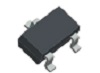
| Type number | Package | Packing | Product status | Marking | Orderable part number | Ordering code (12NC) |
|---|---|---|---|---|---|---|
| ESDALD05BE2 |
SOT23-3L |
STANDARD MARK SMD | Volume production | Standard Marking | ESDALD05BE2X | 9340 730 86115 |
| Type number | Ordering code (12NC) | Orderable part number | Region | Distributor | Order sample |
|---|---|---|---|---|---|
| ESDALD05BE2 | 9340 730 86115 | ESDALD05BE2X | NA | NA |
| Chemical content | Orderable part number | Type number | RoHS / RHF | Leadfree conversion date | MSL | MSL LF |
|---|---|---|---|---|---|---|
| ESDALD05BE2 | ESDALD05BE2X | ESDALD05BE2 |  |
always Pb-free | 1 | 1 |
Disclaimer
All information in this document is furnished for exploratory or indicative purposes only. All information in this document is believed to be accurate and reliable. However, WeEn Semiconductors does not give any representations or warranties as to the accuracy or completeness of such information and shall have no liability for the consequences of use of such information. WeEn Semiconductors may make changes to information published in this document at any time and without notice. Minor deviations may occur in the products from different manufacturing location. This document supersedes and replaces all information supplied prior to the publication hereof. Nothing in this document may be interpreted or construed as an offer to sell products that is open for acceptance or the grant, conveyance or implication of any license under any copyrights, patents or other industrial or intellectual property rights.