
The power we use to run electrical appliances, satiate our growing obsession with generating, processing and consuming data, and support mobility for work and pleasure comes at the cost of a trade-off with the habitable environment. As the effects of this unwelcome exchange become increasingly immediate, government and industry alike are responding with regulations and standards aimed at reigning in energy consumption and shifting toward renewable energy sources.
While individually each of the applications like HVAC, datacenter servers, solar and wind power storage, and electric vehicle (EV) fast chargers and traction inverters, have specific design requirements, the common trends of high efficiency, high power density, and lower cooling requirements are dominant for them all.
For instance, datacenters are estimated by the International Energy Agency (IEA) to have consumed anywhere between 200 TWh and 250 TWh in 2020 or about one percent of the global electricity demand. As the global internet traffic shot up by over 40% last year with expectations of continued growth, the U.S. is using the Energy Act (2020) to formalize a government-industry joint effort to increase energy efficiency at federal government datacenters and, eventually, across the industry. In Europe, major datacenter operators have signed the Climate Neutral Data Centre Pact to achieve climate neutrality by 2030. And these efforts are supported by high efficiency requirements of about 96% at half-load and about 91% at full-load from Energy Star’s 80 Plus Titanium certification as well as Ecodesign in Europe (ErP) Lot 9 regulation.
In the range-anxious EV market, efficiency is a synonym for success. Fast charging is another, as it reduces the time spent at the charging station. Car makers are therefore moving toward the 800 V EV bus, which enables them to deliver higher power to the battery without increasing current and, therefore, without increasing the size and weight of copper used in EVs.
In the renewable energy market, where solar panels themselves are not known for efficiency, lower loss in the power electronics is equally precious.
Power density without significant trade-off toward cumbersome cooling systems is important to datacenters, solar power plants and EV charging stations not only because space costs but because smaller, lighter systems are easier, faster and cheaper to install.
This tall order for converters, inverters and all types of power supplies means that they should be able to:
- Switch at high frequency in order to decrease the size, weight and cost of the inductors.
- Have low losses to improve both system efficiency and lower the size, weight and cost of the cooling requirement.
- Be able to tolerate higher temperatures without sacrificing overall power density to cooling requirements.
- Support higher power/voltages needed to reduce system I2R losses.
The necessary semiconductor technology
Where silicon (Si) fails to achieve the specifications needed, silicon carbide (SiC)-based components, such as Schottky diodes and MOSFETs, enable applications with a significantly lower energy impact. This is because SiC is a wide bandgap semiconductor that has:
- A much lower ON-state voltage drop, which reduces conduction losses, and lower OFF-state leakage currents than Si.
- Higher edge rates during switching, thus lower switching losses.
- Higher breakdown field that allows higher voltages and a much higher thermal conductivity that allows devices to cool faster.
- Robustness against temperature, thus lowering cooling requirements.
This is the reason the use of SiC diodes and MOSFETs in power electronics is growing rapidly. Market research firm Omdia expects the wide bandgap (GaN and SiC) discrete market share to increase from 5% in 2020 to 17% in 2024, growing at nearly 4.4% CAGR.
Although SiC Schottky diodes have been used in power applications for a couple of decades, the device design and manufacturing technology have continued to evolve and contribute to this growth. For instance, the U.S. Department of Energy’s Solar Energy Technologies Office (SETO) has a funding program to examine issues related to efficiencies in generating, distributing and storing solar energy. It counts as participants both companies developing SiC-based high-voltage converters and string inverters, as well as university research teams working on SiC technologies.
In the EV area, Yole Développement estimates power SiC devices in EV/HEV will grow beyond $1.5 billion in 2025 at a CAGR during 2019-2025 of 29 percent. SiC is being used in several EV systems, including the traction inverter, the DC-DC converter, the on-board charger, as well as fast-charging (off-board) infrastructure that tackles the last barrier to widespread EV acceptance.
WeEn: the key supplier of a key technology
WeEn Semiconductors addresses this market demand for SiC components with SiC Schottky diodes. The company has a 50-year history in power-device development and manufacturing, starting as an effort by Philips, then NXP before being spun off as WeEn Semiconductors in 2015 armed with a merged PiN Schottky (MPS) technology for manufacturing SiC Schottky diodes.
Based in China, the company now has a global footprint comprising two R&D centers, two application laboratories, one reliability and failure analysis laboratory, 10 WeEn corporate entities, 12 sales offices, and six representative offices together employing 350 staff worldwide.
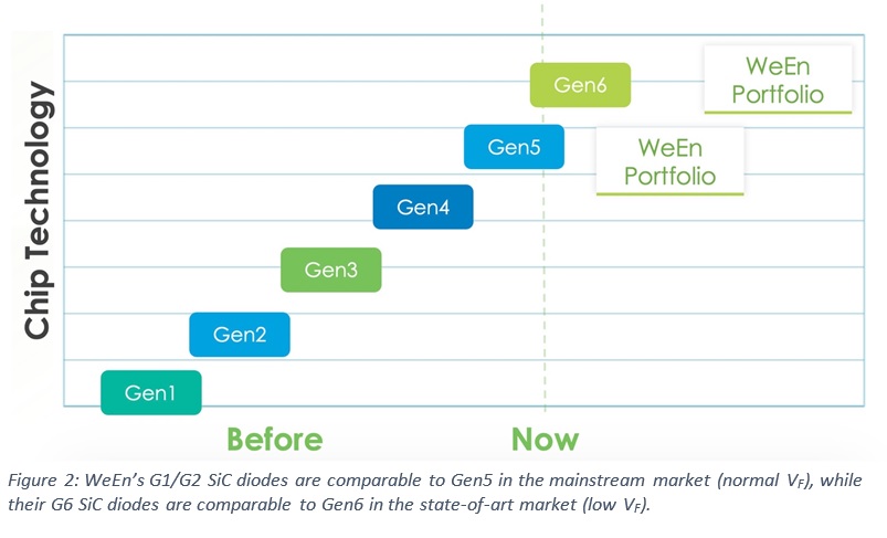
In 2017, WeEn finished transferring production from the older 100-mm wafer line to a 150-mm line to match an increasing demand. In 2019, the company became one of the pioneers in moving beyond the fifth generation SiC Schottky diode technology to the sixth generation that makes it easier for designers to meet the latest efficiency standards mentioned earlier.
WeEn technology explained
The MPS technology builds on the Junction Barrier Schottky (JBS) concept that uses P islands in the N- epitaxial layer to move the peak in the reverse-mode electric field away from the Schottky layer, thereby reducing reverse leakage current and attendant losses. An MPS diode introduces relatively larger P+ regions in the N- epitaxial layer connected through ohmic contacts.
This combines the low forward voltage advantage typical of the SiC Schottky diode with the better inrush current handling of the PiN diode. At high forward current density or a surge, the PN junction in the MPS structure injects minority carriers in the drift region of the diode thereby lowering the forward voltage drop at high current density.
Increasing the PN area means reducing the Schottky area, which increases ON-resistance at nominal forward current. WeEn addresses this by using proprietary low-resistance ohmic contacts to the P+ region to reduce the overall ON-resistance. WeEn SiC MPS diodes thus have better surge current handling than competing parts without trading off current conduction capability.
The company has further developed device technology, reducing the N+ substrate thickness by “back-grinding” such that the resulting wafer thickness is only one-third that of standard chips on the market. The wafer thinning significantly reduces the contribution of the substrate to the total ON resistance. It also results in a much lower thermal resistance so that a lowering of junction temperature by as much as 50°C is achieved.
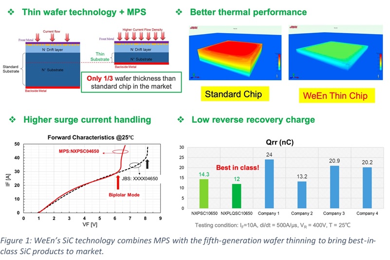
WeEn SiC parts are also best-in-class in terms of the reverse recovery charge, Qrr. The temperature-independent low Qrr allows designers to use WeEn Schottky parts in high-frequency switching applications, such as power factor correction (PFC) circuits that can switch up to 140 kHz. Moreover, the parts are qualified up to junction temperatures of 175°C.
These characteristics address the previously discussed high efficiency and power density, and low cooling requirements from applications today.
Roadmap to efficiency
WeEn’s older generation offerings are comparable to fifth-generation products in the mainstream market but with better surge current handling. Their latest G6 products with ultra-low VF are comparable to competing Gen.6 products but with significantly lower junction-to-case thermal resistance and therefore higher current handling capability.
The compelling benefits of SiC devices has increased their adoption with EV on-board charger and traction, as well as charging infrastructure markets expected to grow rapidly. Yole Développement expects the automotive segment to capture as much as 60 percent of the SiC market share in 2026.
WeEn therefore continues to develop not only its SiC technology and but higher-performance packages. Its recently launched automotive qualified (AECQ-101) is a testament to future product development focus. The company is working to expand its 650-V and 1200-V Schottky diode portfolio to 1700 V and has planned 1200-V MOSFETs as well as MOSFET modules in its technology roadmap.
To find a part that suits your design, see WeEn Semiconductors’ product portfolio here.